IGBT – Working, Types, Structure, Operation & Applications
Thyristors are the most used components in modern electronics and logic circuits are used for switching and amplification. BJT and MOSFET are the most used types of the transistor where each of them has its own advantage over the other and some limitations. The IGBT (Insulated Gate Bipolar Transistor) takes the best parts of both BJT and MOSFET into a single transistor. It takes the input characteristics (high input impedance) of MOSFET (Insulated Gate) and the output characteristics of BJT (Bipolar nature).
- Related Post: GTO – Types, Construction, Working and Applications
Table of Contents
What is IGBT?
The IGBT or Insulated Gate Bipolar Transistor is the combination of BJT and MOSFET. Its name also implies the fusion between them. “Insulated Gate” refers to the input part of MOSFET having very high input impedance. It does not draw any input current rather it operates on the voltage at its gate terminal. “Bipolar” refers to the output part of the BJT having bipolar nature where the current flow is due to both types of charge carriers. It allows it to handle very large currents and voltages using small voltage signals. This hybrid combination makes the IGBT a voltage-controlled device.
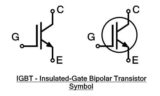
It is a four-layer PNPN device having three PN junctions. It has three terminals Gate (G), Collector(C) and Emitter (E). The terminal’s name also implies being taken from both transistors. Gate terminal as it is the input part, taken from MOSFET while the collector and emitter as they are the output, taken from the BJT.
Related Post:
- DIAC – Construction, Working and Applications
- TRIAC – Construction, Working and Applications
Construction of IGBT
IGBT is made of four layers of semiconductor to form a PNPN structure. The collector (C) electrode is attached to P layer while the emitter (E) is attached between the P and N layers. A P+ substrate is used for the construction of IGBT. An N- layer is placed on top of it to form PN junction J1. Two P regions are fabricated on top of N- layer to form PN junction J2. The P region is designed in such a way to leave a path in the middle for the gate (G) electrode. N+ regions are diffused over the P region as shown in the figure.
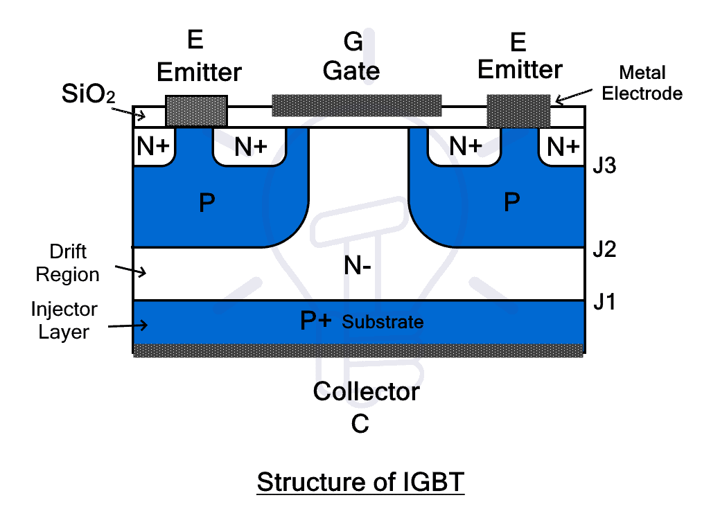
The emitter and gate are metal electrodes. The emitter is directly attached to the N+ region while the gate is insulated using a silicon dioxide layer. The base P+ layer inject holes into N- layer that is why it is called injector layer. While the N- layer is called the drift region. Its thickness is proportional to voltage blocking capacity. The P layer above is known as the body of IGBT.
The N- layer is designed to have a path for current flow between the emitter and collector through the junction using the channel that is created under the influence of the voltage at the gate electrode.
- Related Post: What is the Difference Between DIAC and TRIAC?
Equivalent Structure of IGBT
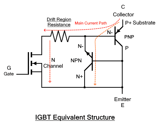
As we know that IGBT is the combination of input of MOSFET and output of BJT, it has an equivalent structure to N-channel MOSFET and a PNP BJT in Darlington configuration. The resistance of the drift region can also be incorporated.

If we look at the structure of the IGBT above, there is more than one path for the current to flow. The current path is directed from collector to emitter. The first path is “collector, P+ substrate, N-, P, emitter”. This path is already mentioned using the PNP transistor in an equivalent structure. The 2nd path is “collector, P+ substrate, N-, P, N+, emitter”. To include this path, another NPN transistor must be included in the structure as shown in the figure below.
Working of IGBT
The two terminals of IGBT collector (C) and emitter (E) are used for the conduction of current while the gate (G) is used for controlling the IGBT. Its working is based on the biasing between Gate-Emitter terminals and Collector-Emitter terminals.
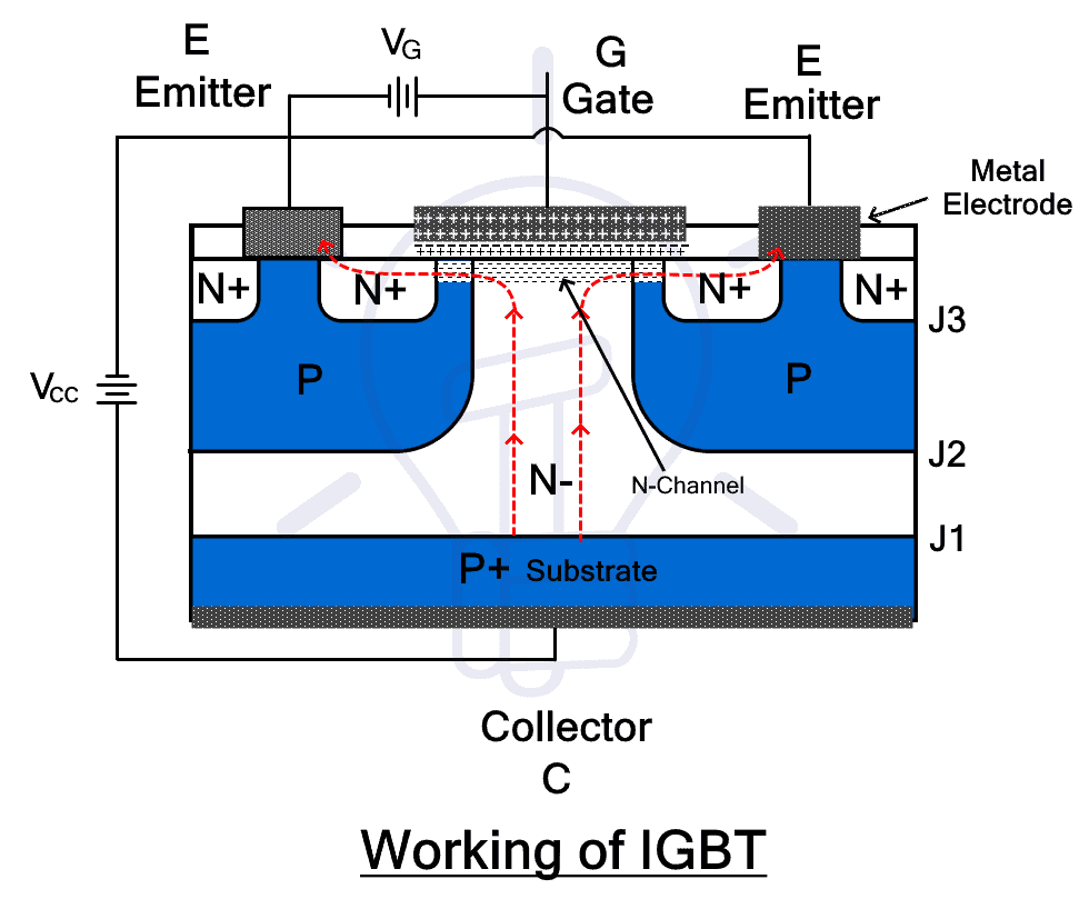
The collector-emitter is connected to Vcc such that the collector is kept at a positive voltage than the emitter. The junction j1 becomes forward biased and j2 becomes reverse biased. At this point, there is no voltage at the gate. Due to reverse j2, the IGBT remains switched off and no current will flow between collector and emitter.
Applying a gate voltage VG positive than the emitter, negative charges will accumulate right beneath the SiO2 layer due to capacitance. Increasing the VG increases the number of charges which eventually form a layer when the VG exceeds the threshold voltage, in the upper P-region. This layer form N-channel that shorts N- drift region and N+ region.
The electrons from the emitter flow from N+ region into N- drift region. While the holes from the collector are injected from the P+ region into the N- drift region. Due to the excess of both electrons and holes in the drift region, its conductivity increase and starts the conduction of current. Hence the IGBT switches ON.
- Related Post: Types of Transistors – BJT, FET, JFET, MOSFET, IGBT & Special Transistors
Types of IGBT
There are two types of IGBT based on the inclusion of N+ buffer layer. The inclusion of this extra layer divides them into symmetrical and asymmetrical IGBT.
Punch through IGBT
The Punch through IGBT includes N+ buffer layer due to which it is also known as an asymmetrical IGBT. They have asymmetric voltage blocking capabilities i.e. their forward and reverse breakdown voltages are different. Their reverse breakdown voltage is less than its forward breakdown voltage. It has faster switching speed.
Punch through IGBTs is unidirectional and cannot handle reverse voltages. Therefore, they are used in DC circuits such as inverters and chopper circuits.
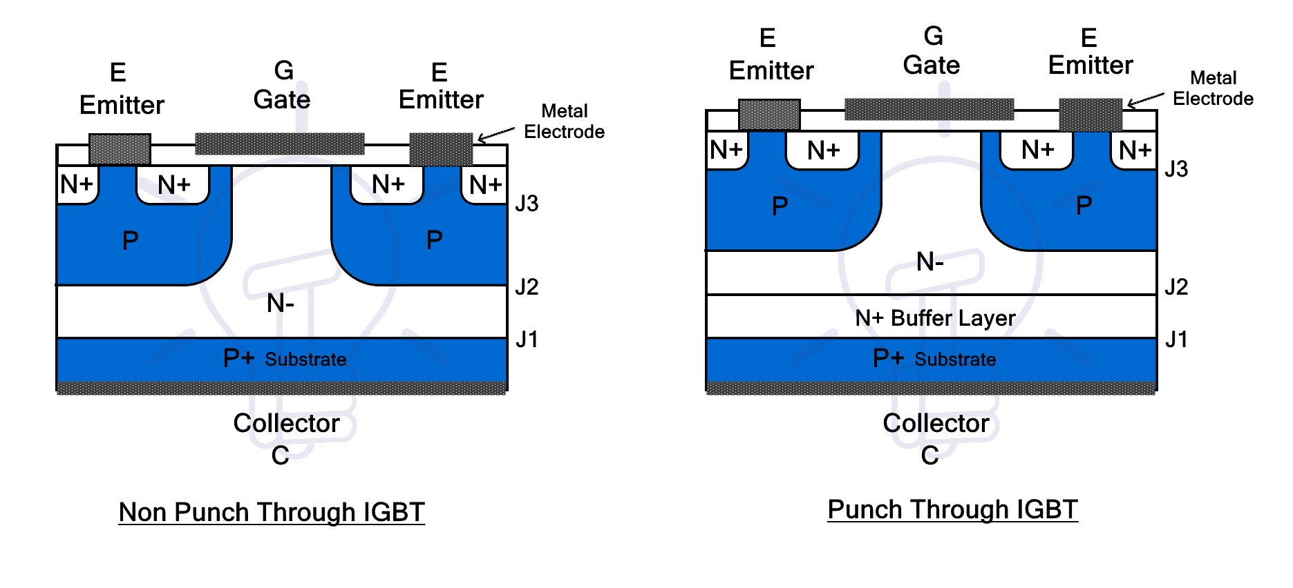
Non Punch through IGBT
They are also known as symmetrical IGBT due to the absence of extra N+ buffer layer. The symmetry in structure provides symmetrical breakdown voltage characteristics i.e. the forward and reverse breakdown voltages are equal. Due to this reason, they are used in AC circuits.
V-I Characteristics of IGBT
Unlike BJT, IGBT is a voltage-controlled device that requires only a small voltage at its gate to control the collector current. However, the gate-emitter voltage VGE needs to be greater than the threshold voltage.
Transfer characteristics of the IGBT show the relation of input voltage VGE to output collector current IC. When the VGE is 0v, there is no IC and the device remains switched off. When the VGE is slightly increased but remains below threshold voltage VGET, the device remains switched off but there is a leakage current. When the VGE exceeds the threshold limit, the IC starts to increase and the device switches ON. Since it is a unidirectional device, the current only flows in one direction.

The given graph shows the relation between the collector current IC and collector-emitter voltage VCE at different levels of VGE. At VGE < VGET the IGBT is in cutoff mode and the IC = 0 at any VCE. At VGE > VGET, the IGBT goes into active mode, where the IC increases with an increase in VCE. Furthermore, for each VGE where VGE1 < VGE2 < VGE3, the IC is different.
The reverse voltage should not exceed the reverse breakdown limit. So does the forward voltage. If they exceed their respective breakdown limit, uncontrolled current starts passing through it.
General Comparison with BJT and MOSFET
As we have discussed above, IGBT takes the best parts of both BJT and MOSFET. Therefore, it is superior in almost every way. Here is a chart of some of the characteristics showing the comparison between IGBT, BJT and MOSFET. we are comparing power devices in their max capabilities.
| Characteristic | Power BJT | Power MOSFET | IGBT |
| Voltage Rating | High < 1kV | High < 1kV | Very High > 1kV |
| Current Rating | High < 500 A | Low < 200 A | Very High > 500 A |
| Input Parameter | Base Current, Ib | Voltage, VGS | Voltage, VGE |
| Input Drive | Current gain (hfe)
20-200 |
Voltage, VGS 3-10V |
Voltage, VGE
4-8V |
| Input Drive Power | High | Low | Low |
| Input Drive Circuitry | Complex | Simple | Simples |
| Input Impedance | Low | High | High |
| Output Impedance | Low | Medium | Low |
| Switching Loss | High | Low | Medium |
| Switching Speed | Low | Fast | Medium |
| Cost | Low | Medium | High |
Advantages & Disadvantages of IGBT
Advantages
IGBT as a whole has the advantages of both BJT and MOSFET.
- It has higher voltage and current handling capabilities.
- It has a very high input impedance.
- It can switch very high currents using very low voltage.
- It is voltage-controlled i.e. it has no input current and low input losses.
- The gate drive circuitry is simple and cheap.
- It can be easily switched ON by applying positive voltage and OFF by applying zero or slightly negative voltage.
- It has very low ON-state resistance
- It has a high current density, enabling it to have a smaller chip size.
- It has a higher power gain than both BJT and MOSFET.
- It has a higher switching speed than BJT.
Disadvantages
- It has a lower switching speed than MOSFET.
- It is unidirectional it cannot conduct in reverse.
- It cannot block higher reverse voltage.
- It is costlier than BJT and MOSFET.
- It has latching problems due to the PNPN structure resembling thyristor.
Applications of IGBT
IGBTs have numerous applications used in AC as well as DC circuits. Here are some of the important applications of IGBT
- It is used in SMPS (Switched Mode Power Supply) to supply power to sensitive medical equipment and computers.
- It is used in UPS (Uninterruptible Power Supply) system.
- It is used in AC and DC motor drives offering speed control.
- It is used in chopper and inverters.
- It is used in solar inverters.
Related Posts:
- What are Thyristor and SCR? Types, Working and Applications
- What is Rectifier? Types of Rectifiers and their Working Principle
- What is MOSFET? Working, Types, Operation, and Applications
- What is Diode? Construction & Working of PN Junction Diode
- What is BJT? Construction, Working, Types and Applications


Thank you. Keep up the good work